Solder pads are the basic building blocks of surface mounted assembly on PCBs. As an excellent PCB engineer, having a rich knowledge reserve of solder pads is essential. Many people can draw solder pads by following component manuals, but it is important to pay attention to how to draw the best solder pads. Here are some tips that will help you learn more about solder pad knowledge.

Types of solder pads
In general, solder pads can be divided into six major categories based on their shape, as follows:
- Square pads – widely used in printed boards where components are large and few, and printed wiring is simple. This type of pad is easy to implement by hand in PCB manufacturing.
- Round pads – commonly used in single- and double-sided printed boards where components are regularly arranged. If the board density allows, the pads can be larger to prevent detachment during soldering.
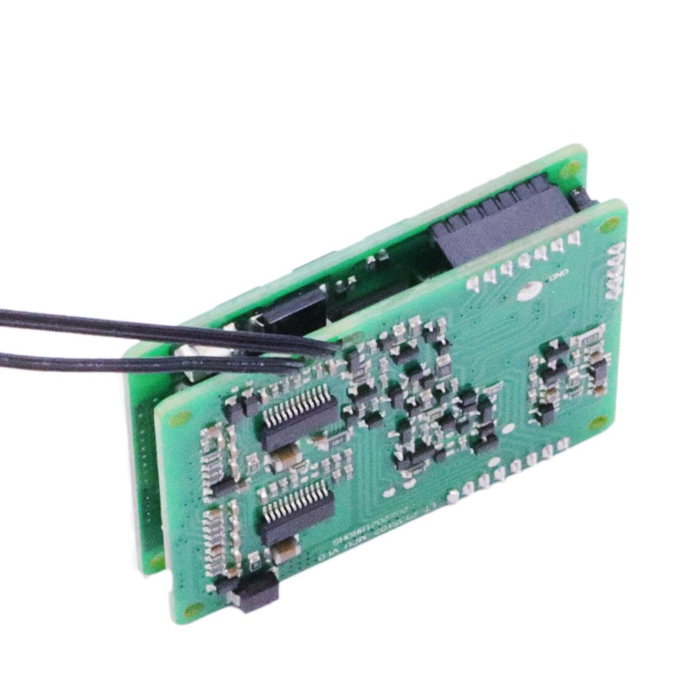
- Island-shaped pads – the connection between pads and pads is integrated into one. This type of pad is commonly used in vertical irregular arrangements. For example, it is often used in audio players.
- Tear-shaped pads – used when the wire connected to the pad is relatively thin to prevent the pad from peeling and the wire from detaching from the pad. This type of pad is commonly used in high-frequency circuits.
- Polygonal pads – used to distinguish pads with different outer diameters but the same inner diameter for easy processing and assembly.
- Ellipse-shaped pads – this type of pad has enough area to enhance pull resistance and is commonly used in dual-inline straight devices.
- Open-shaped pads – this type of pad is commonly used to prevent the manual welding pad hole from being sealed by solder after wave soldering.
Design standards for solder pad shapes and sizes in PCB design
- All solder pads should have a minimum side length of no less than 0.25mm, and the maximum diameter of the entire pad should not exceed three times the diameter of the component hole.
- Efforts should be made to ensure that the spacing between the edges of two solder pads is greater than 0.4mm.
- In cases where the wiring is dense, oval and long rectangular connecting pads are recommended. The minimum width or minimum diameter of a single-sided connecting pad should be 1.6mm; for double-sided weak current circuits, the pad only needs to be 0.5mm larger than the hole diameter. Pads that are too large may cause unnecessary welding, and the hole diameter should not exceed 1.2mm or the pad diameter should not exceed 3.0mm. Pad design should be diamond or plum blossom-shaped for these cases.
- For inserted components, to avoid copper foil breakage during soldering and ensure complete coverage of the single-sided connecting pad by copper foil; for double-sided components, solder droplets should be added at the smallest requirements to tears.
- All machine-inserted components require designing drop tears on the welding points along the bending direction to ensure that the welding points at the bending point are full.
- The welding pads on the large area of copper foil should be designed as a chrysanthemum-shaped pad to avoid false welding. If there is a large area of ground lines and power lines on the PCB (greater than 500 square millimeters), it should be partially opened or designed as a grid filling.
Requirements for solder pads in PCB manufacturing processes
- Connecting pads for surface mounted components at both ends of an IC that do not connect to manually inserted component pads should be provided with test points. The test point diameter should be equal to or greater than 1.8mm to facilitate in-line testing by an inspection machine.
- If there are no connecting pads for dense IC pins on the PCB, test pads need to be added, especially for surface mounted ICs, test points cannot be placed within the surface mounted IC silkscreen print area. The test point diameter should be equal to or greater than 1.8mm to facilitate in-line testing by an inspection machine.
- If the pad spacing is less than 0.4mm, white oil needs to be applied to reduce soldering together during wave soldering.
- If there are hand-soldering components on a single-sided board, a walk tin slot should be provided opposite to the direction of tin waves and with a width of 0.3mm to 1mm according to the size of the hole.
- The size and spacing of solder pads for surface mounted components should match the actual size of the surface mounted components exactly.